
![]()
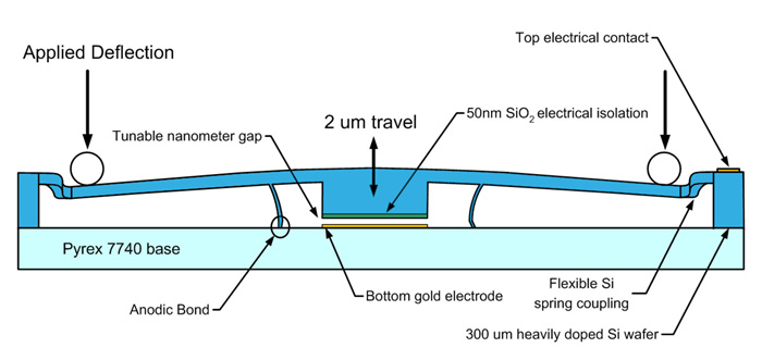
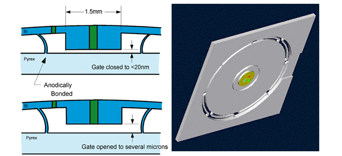
The nanogate is a micro electromechanical systems (MEMS) device capable of accurately and repeatably controlling the separation of a nanometer gap between two very flat surfaces. The nanometer gap is achieved using a lever-fulcrum structure made from patterned silicon and Pyrex wafers adhered to each other via anodic bonding. The lever-fulcrum structure is circular (see 3D Pro/Engineer model below) and when a force is applied to the outside edge the central region can be opened in very small increments with a certain transmission ratio. The nanogate was originally developed by Alex Slocum's Precision Engineering Research Group, here's their web site on the nanogate.
Several unique characteristics of the nanogate may lead to important commercial and scientific applications:
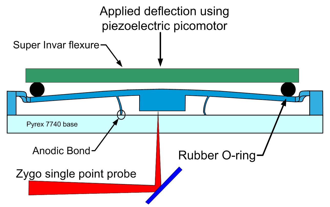
In fall of 2001, James White and Hong Ma designed an experimental setup to test an initial version of the nanogate. The nanogate was actuated through a spring flexure using a piezoelectric motor. The piezoelectric motor drove a lead screw that advanced in submicron steps depending on the amount of loading. The displacement of the center region is measured using a single point Michelson interferometer from Zygo Corporation. All the mechanical interfacing components including the flexure are made of Super Invar, a material designed with the lowest possible thermal expansion coefficient at room temperature.
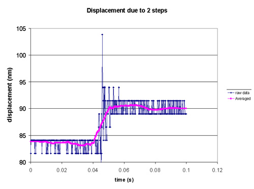
Some results from the first experiment with deflecting the nanogate. It looks like we can control the gap opening to in 4.5 nm increments. Our interferometer had a measurement resolution of 2.4 nm.
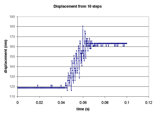
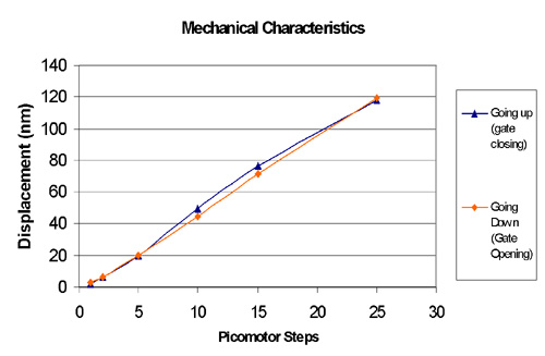
Total mechanical response looks pretty good. It looks like it the actuator needs one wasted step to get going. We think the deviation from "going up" vs. "going down" comes from thermal drifts that happened while we were taking data.
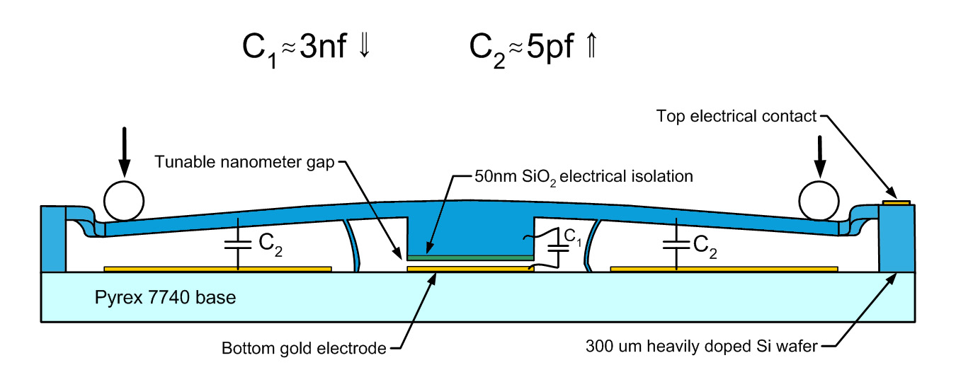
Currently, we are attempting to measure displacement using capacitance. The most straight forward technique is to measure capacitance of the center region. However, this measurement may be unfeasible when we put fluids and various molecules in the nanogap. So we are also exploring measuring displacement on the outside region.
Publications
IEEE Sensors 2003 Conference. This paper won 3rd place out over 300 at the
student paper competition.
Sub-nanometer Displacement Sensing for the Nanogate, Ma, H., White, J.,
Paradiso, J., and Slocum, A. In the Proceedings of the 2003 IEEE
International Conference on Sensors, Oct. 21-24.
For more information on this project please contact: Hong Ma at hongma (at) media.mit.edu
Return to the Responsive Envirionments Group